|
Contact us

Connecting technologyDriving innovation

FUTENG TECHNO

Glass-based Advanced Packaging & AI Computing Infrastructure

From glass materials, TGV and RDL to pilot manufacturing and AI engineering compute — a technology platform built for next-generation high-performance computing.

Next-gen packaging
for AI / HPC
Materials × Process
× Equipment
From R&D to
industrialization
Serving global
markets
SCROLL DOWN
30+yrs
Core team semiconductor experience
510 × 515mm
Panel-level pilot platform roadmap
GI · GCS · 3D
Three product & technology lines
2017
Founded in Singapore

COMPANY PROFILE · EST. 21 APR 2017

Built on industry service, scaling advanced packaging and AI computing

Founded on 21 April 2017 in Singapore, FUTENG is a semiconductor industry service and R&D company providing equipment, materials, technical consulting and training. We are developing glass-based advanced packaging, with phased AI computing infrastructure as an independent strategic expansion.

  • Materials & spare parts
  • Semiconductor equipment
  • Pre-owned & refurbished tools
  • Technology commercialization
  • Training & technical support
Existing businessTechnology upgradeTwo growth engines
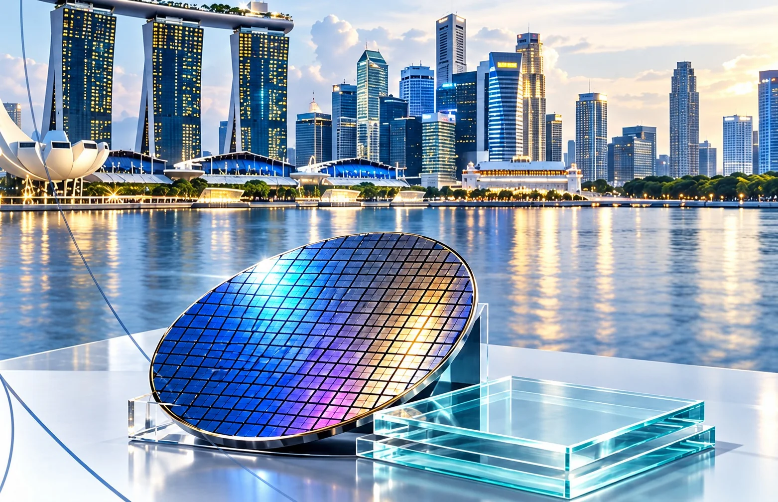
新加坡滨海湾与晶圆、玻璃基板
SingaporeHeadquarters · Connecting the semiconductor industry

Two strategic pillars

Two strategic pillars

TECHNOLOGY DRIVES INDUSTRY · EMPOWERING A SMARTER FUTURE

01

Glass-based Advanced Packaging

Glass-based advanced packaging
Next-generation packaging for the AI / HPC era
  • Glass material & process development
  • TGV & metallization
  • Multi-layer RDL & advanced packaging
  • Pilot manufacturing & process validation
Learn more
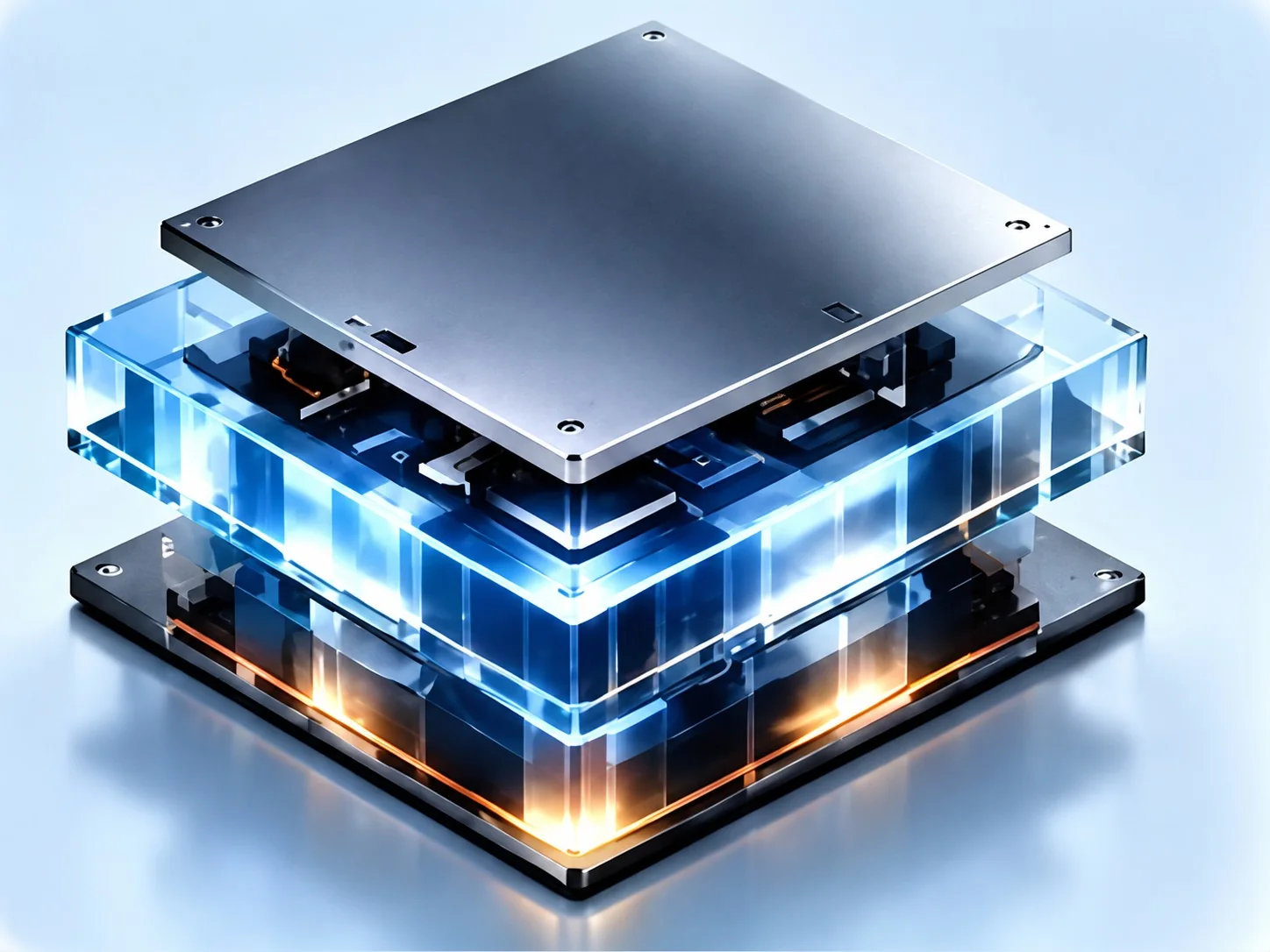
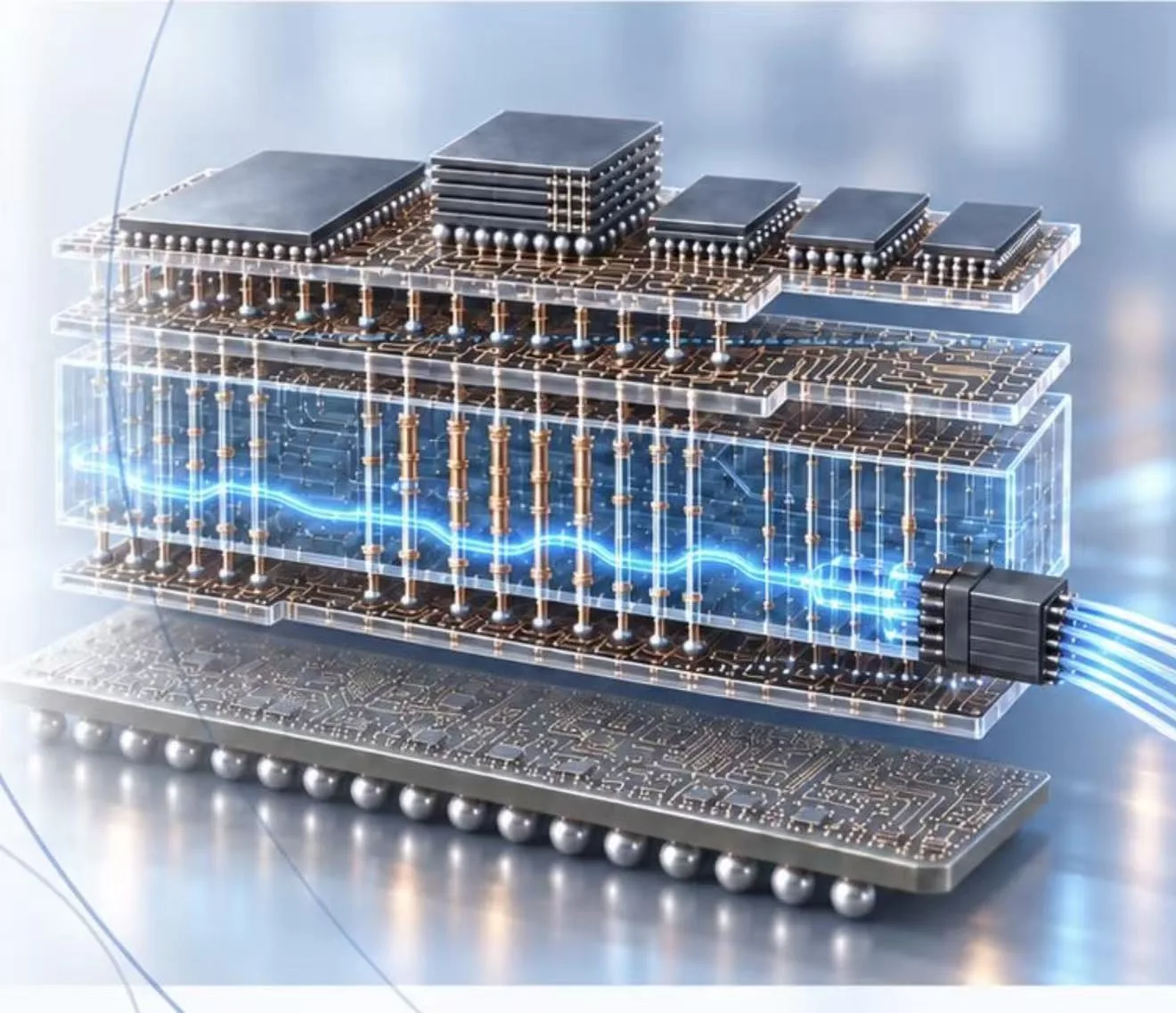
玻璃基多层互连结构
02

AI Computing Infrastructure

AI computing infrastructure plan
An independent, phased expansion for enterprise AI / HPC
  • Phased targets: 64 → 128 → 192 servers
  • Cumulative deployment target: 256 servers
  • Final hardware selected at procurement
  • IDC location & hosting partner under evaluation
Learn more
Strategic ExpansionAI 服务器机房

Advanced packaging technologies

Advanced packaging technologies

Explore key packaging approaches for high-performance computing, from chiplet interconnects and vertical stacking to thermal design.

01 · 2.5D

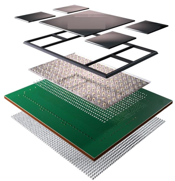
2.5D packaging: chiplet interconnects

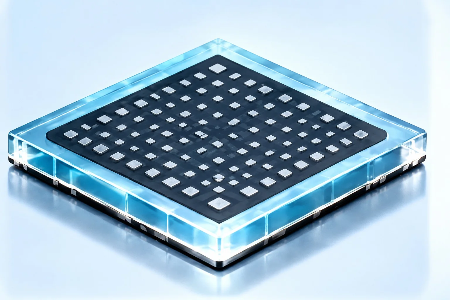
2.5D chiplet, interposer and substrate structure
Technical illustration · View original ↗

An interposer connects multiple chiplets and integrates them with a package substrate, forming a chiplet–interposer–substrate structure.

  • Chiplet types include ASICs, xPUs, HBM and HBF.
  • Interposer options include silicon, organic materials and RDL, with embedded capacitors and integrated passive devices (IPD).
  • Substrate design involves thick cores, low-dielectric-constant materials and bump-based interconnects.

02 · 3D

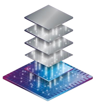
3D packaging: vertical chip stacking

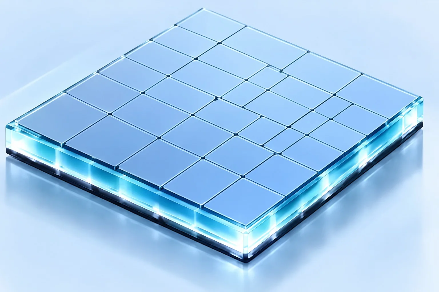
3D vertical chip stacking structure
Technical illustration · View original ↗

Chips are integrated vertically, using microbumps or hybrid bonding to create interconnections between layers.

  • Stacking structures include logic-on-logic and logic-on-memory, including SRAM and DRAM.
  • Interconnect options include microbumps (μbump) and hybrid bonding.
  • Integration approaches include Die-on-Wafer and Wafer-on-Wafer, with face-to-face or face-to-back structures.

03 · 3.5D

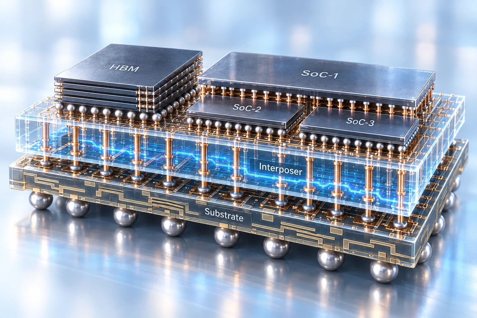
3.5D integration: stacking meets interconnects

3.5D stacked SoC and HBM interposer cross-section
3D concept illustration · View full size ↗

Combines 3D chip stacking with 2.5D packaging, bringing vertical integration and lateral interconnects into one package.

  • Hybrid bonding connects vertically stacked chips.
  • An interposer connects the stacked chips laterally with chiplets such as HBM.
  • The combined chip and interposer structure then connects to the package substrate.

04 · THERMAL

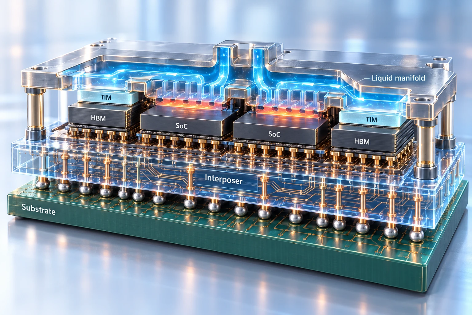
Thermal design: materials and microchannels

Microchannel cooling cross-section with liquid manifold
3D concept illustration · View full size ↗

Combines high-thermal-conductivity materials with microchannel cooling structures across chips, lids and their interfaces.

  • Material approaches include silicon carbide (SiC) substrates, microcrystalline or nanocrystalline diamond films, and copper–diamond composites.
  • Microchannels can be integrated inside the heat-spreader lid.
  • Cooling paths can also integrate structures within both silicon and the lid.

These descriptions introduce technology approaches. FUTENG’s glass-based process platform and product roadmap follow below.

Technology platform

Technology platform

From materials to systems: an advanced process platform for HPC, heterogeneous integration and co-packaged optics.

01
Glass MaterialGlass Material
02
Ultrafast LaserLaser / SLE
03
TGVThrough Glass Via
04
Barrier / SeedBarrier / Seed Layer
05
MetallizationMetallization
06
CMPChemical Mechanical Polishing
07
Multi-layer RDLMulti-layer RDL
08
AssemblyAssembly
09
ReliabilityReliability

Product roadmap

Product roadmap

Built on glass materials and panel-level processing, from process validation to product introduction.
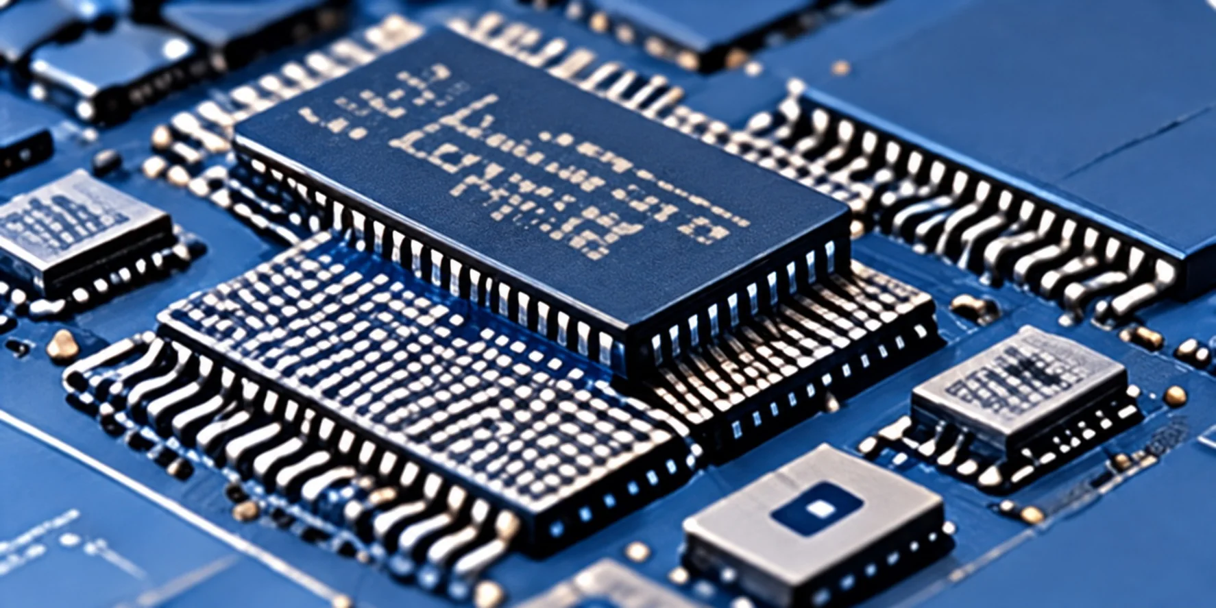
GI 玻璃中介层
Current lead product
GI Glass Interposer
Glass Interposer (GI)

Multi-die interconnect for AI/HPC, HBM, chiplets and advanced packaging.

GCS 玻璃核心基板
Independent product line
GCS Glass Core Substrate
Glass Core Substrate (GCS)

For high-density packaging and large-format substrates.

三维光电集成
Mid-to-long-term R&D
3D Optoelectronic Integration

For CPO, silicon photonics and electro-optical integration.

Technology maturity & scale-up path
Months from project start (M); phases overlap
P0-AMechanism / material / coupon validation
M1–M9
P0-B510×515 mm full-panel validation
M7–M18
P1Controlled pilot production · customer co-development
M13–M36
P2 / Scale-UpAdvanced integration / CPO · scale-up preparation
M37–M60
M0M12M24M36M48M60

AI Computing Infrastructure Plan

AI computing infrastructure plan

MORE COMPUTE. A SMARTER TOMORROW.

Planned for Malaysia as an independent commercial project alongside glass-based manufacturing. The four-stage roadmap targets 256 servers cumulatively, with investment and deployment aligned to customer demand.

Advanced AI / HPC
server configurations
IDC location
under evaluation
Security & compliance
by design
Phased investment
aligned to demand
Discuss the deployment plan
INDICATIVE ROADMAP · CUMULATIVE SERVER TARGETS
Phase 1
Initial deployment
64units
AI servers

Initial capacity, subject to project readiness

Phase 2
Capacity expansion
128units
AI servers

Expand capacity with validated demand

Phase 3
Business expansion
192units
AI servers

Scale with business development

Final scale
Cumulative target
256units
AI servers

Long-term deployment target

Planning targets, not installed capacity. The specific IDC location and hosting provider remain to be selected. GB300 is a provisional reference; final equipment, timing and scale depend on procurement configuration, quotations, compliance and project progress.

Why Futeng

Why Futeng

From materials to industrialization, engineering capability that connects technology and industry.

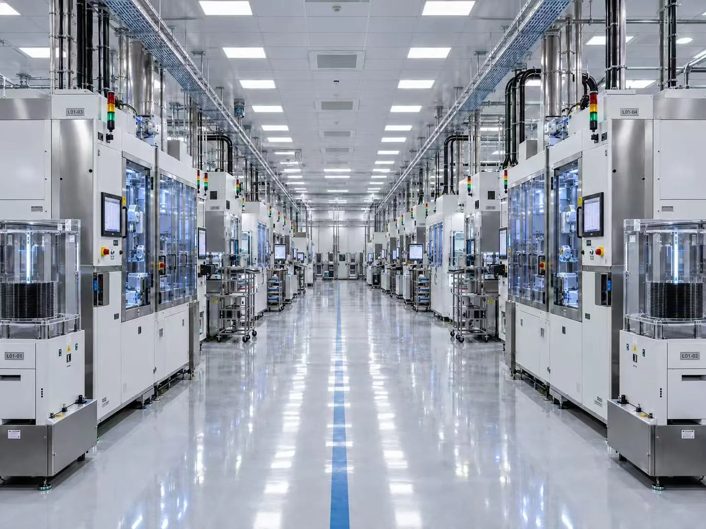
先进封装洁净车间产线示意
ADVANCED PACKAGING · LINE REFERENCEAdvanced packaging production line reference
Engineering Integration

A closed engineering loop: material → TGV → metallization → RDL → reliability.

Pilot Manufacturing
Pilot Manufacturing

Developing a pilot platform for engineering validation and customer qualification.
Multidisciplinary Team

Experts in process, equipment, IC design, materials and industrialization.

Digital Engineering
Digital Engineering

Simulation, process data, yield models and AI optimization.

Leadership & team

Leadership & team

Experience across international business management, semiconductor process, advanced packaging, equipment, IC design, materials, manufacturing and industrial capital.

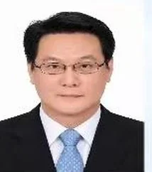
Dr. Alex Zheng

Dr. Alex Zheng

Chairman of the Board of Futeng Technology

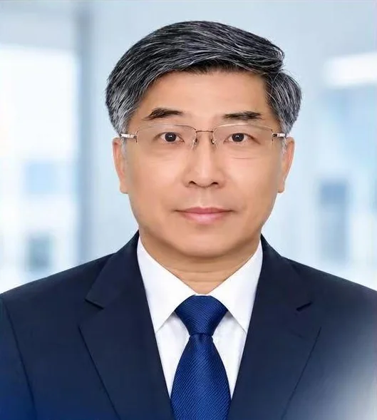
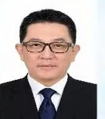
Dr. Alex Zheng holds a DBA and specializes in semiconductor process R&D, operations, and corporate strategy. He has held leadership roles at SMIC, TSMC, and A*STAR's Institute of Microelectronics, and serves as Vice President of Sari Technology and Chairman of the Board of Futeng Technology in Singapore.

Doctor of Business Administration (DBA)
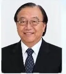
Dr. Francis Koay

Dr. Francis Koay

Chief Executive Officer (CEO)

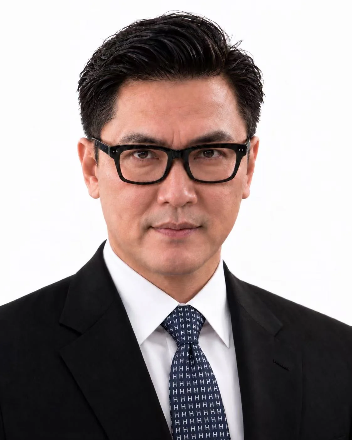
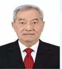
An international defense trade professional with expertise in oil and gas, artificial intelligence, and cybersecurity. He brings extensive experience in international business management, leading research and development teams, and investment, and also serves as a political advisor.

PhD in Law
Bryan Hung

Bryan Hung

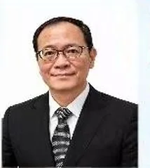
Bryan Hung specializes in semiconductor equipment development and maintenance, production management, and manufacturing process optimization. His experience spans equipment R&D and factory management, with current work focused on semiconductor packaging materials and process waste recycling.

Joe Hung

Joe Hung

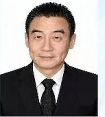
Joe Hung specializes in LED and MicroLED display technologies, advanced semiconductor packaging, and process materials. He has held management roles in Foxconn's display and semiconductor businesses and is a founding shareholder of GPTC and founder of Tech-point in Taiwan and Singapore.

Dr. Dongsheng Yang

Dr. Dongsheng Yang

Dr. Dongsheng Yang holds a bachelor's degree in physics from Tsinghua University and a Ph.D. in solid-state and nuclear physics from Rutgers University. His semiconductor R&D and management experience includes roles as Distinguished Member of Technical Staff at Bell Labs, Executive Vice President at Grace Semiconductor, and Chief Scientist at Chongqing Liangjiang Semiconductor Research Institute.

Benson Wang

Benson Wang

Benson Wang specializes in LED displays and lighting manufacturing. His expertise includes production process planning in these fields.

Dr. Fred Huang

Dr. Fred Huang

Dr. Fred Huang holds a Ph.D. in physics from Southern Methodist University and an Executive MBA from Stanford University, with expertise in semiconductor technology, corporate strategy, and venture capital. He has served as CEO of BCD Semiconductor, led Varian's semiconductor business, and held partner roles at Yihe Venture Capital Group and Wuxi Yihe Guolian Investment Management.

Derrick Qiu

Derrick Qiu

Derrick Qiu holds master's degrees in intellectual property and accountancy, with expertise in semiconductor and optoelectronic materials, intellectual property management, and corporate finance. He serves as Founder and General Manager of Hefengding Industrial and General Manager of Shuwei Industrial, and previously served as Vice President at HSBC Singapore.

Luke Lu

Luke Lu

Luke Lu specializes in integrated circuits and advanced packaging. His expertise also includes semiconductor supply chain management.

Ying Shiao

Ying Shiao

Ying Shiao specializes in IC design and manufacturing, display technologies, and advanced semiconductor packaging, with experience in wafer fabrication and supply chain management. Previously Vice President of Operations at eMagin, Ying Shiao serves as Vice President at Operation Fast Power Corporation, overseeing IGBT power semiconductor design and manufacturing.

Partnership & investment

Partnership & investment

We welcome strategic investors, industry partners and key customers to advance validation, deployment and commercialization together.

Equity investment
Equity investment
  • Support the core packaging platform build-out
  • Long-term industrialization value
  • Flexible staged capital contribution
Industrial partnership
  • Synergy in equipment, materials, process and customers
  • Joint validation and sample introduction
  • Long-term ecosystem partnerships
IDC & AI infrastructure
  • Facility, power, cooling and hosting
  • Servers deployed in phases on demand
  • Compute services for enterprise clients
Customer co-development
  • Enterprises, research and public sector
  • Scenario validation and custom solutions
  • Revenue conversion and long-term cooperation
STEP 1NDA & data roomSign NDA and open the data room
STEP 2Technical & commercial DDAssess technology, market and terms
STEP 3Structure & term sheetDefine investment scope and key terms
STEP 4Definitive agreementsSign and launch the first phase

Technology that connects industry

Connecting technology and industry
Empowering a smarter future